

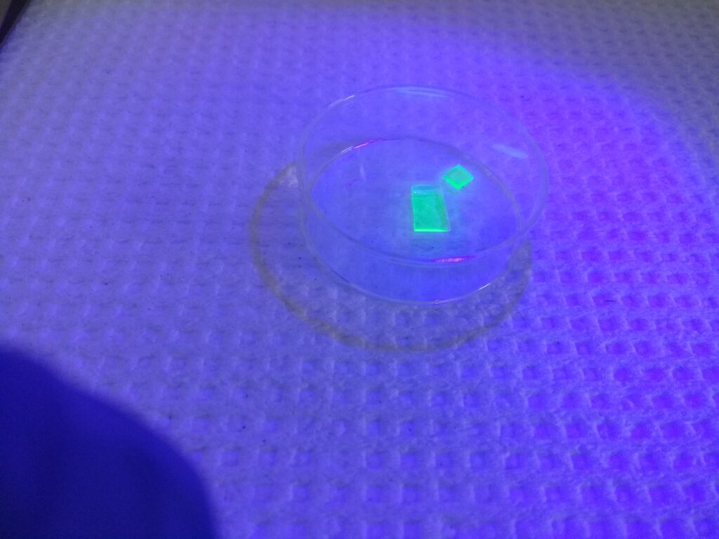
Detectors for X-rays or other high-energy radiation are widely used in medical imaging (X-ray radiology, CT, PET), high energy physics experiments, electron microscopes, image intensifiers, security scanners, and more. In such machines, the radiation detection is done using a scintillation material, which stops the radiation and in a highly non-linear process converts the energy into electron-hole pairs. These electron-hole pairs thermalize and reach luminescence centers and spontaneously recombine into visible light that is then detected with a standard photodetector.
So far, there have been no attempts to improve scintillators by enhancing the intrinsic light-matter interaction process through shaping the photonic modes and their density of states. The process of light emission by the luminescence centers inside the scintillator has always been considered an intrinsic property of the scintillation material, and for example has been considered as essentially isotropic. The isotropy of the emission process reduces the scintillator efficiency as photons that cannot couple out are lost or delayed.
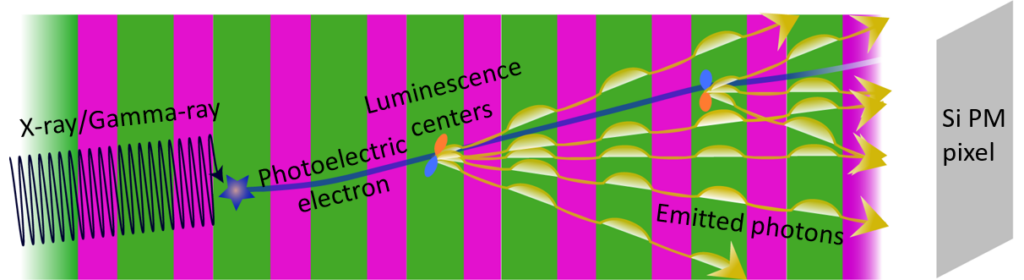
In our lab, we investigate how artificial nanophotonic structure made from a scintillation material can enhance the scintillation efficiency and timing. We propose to design the structure’s geometry on the optical wavelength’s scale to exploit the Purcell effect inside the scintillator. The Purcell effect enables to engineer the optical medium around a point-like, dipole, emitter so that the emission is allowed or inhibited in some directions and frequency ranges. We exemplify this concept with a one-dimensional (1D) periodically patterned optical medium, i.e., a photonic crystal (PhC) structure, made from scintillator materials.
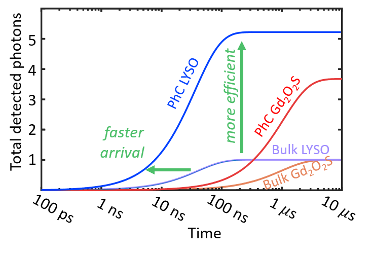
The core effect that enabled the emission rate enhancement, i.e., the Purcell effect, has been already shown in many atomic systems over the years. In such cases, the atomic emitter was located near, or inside, a designed cavity. According to the Purcell effect, the structural design optimization of the cavity can increase the spontaneous emission into the cavity's optical mode, when increasing the quality factor and reducing its volume. However, this design rule cannot be used in our structure, since the detection of the emitted light includes the structure’s efficient outcoupling, which relates to a low quality factor. As a result, we don't optimize our structures to maximize the emission rate in one point, but rather optimize the structure to force as much emission as possible to reach the a nearby photodetector. In the figures below, we show this concept, and the theoretical estimation of many emitted photons can reach the photodetector over time.
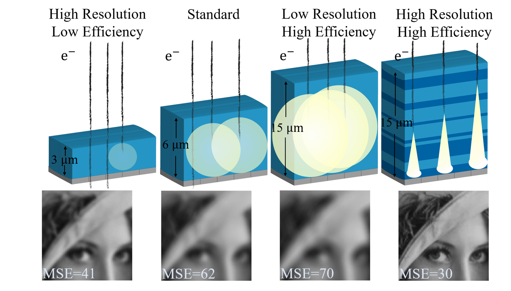
Due to fabrication challenges, the main group of applications that we investigate are Low-energy radiation applications, as light intensifiers, projectional tomography, or particle detectors require only a thin film of scintillation material to stop the radiation. Using analytical formulas, we were able to develop an optimization tool to optimize the multilayer structure to create highly directional scintillation process. The optimization tool enabled to develop a structure with varying layer widths which can improve even further the scintillated signal. In the figure below, we show how an image of a night-vision device can be improved with this concept, overcoming the basic trade-off between resolution and efficiency.
|
|
C. Roques-Carmes, N. Rivera, A. Ghorashi, S. E. Kooi, Y. Yang, Z. Lin, J. Beroz, A. Massuda, J. Sloan, N. Romeo, Y. Yu, J. D. Joannopoulos, I. Kaminer, S. G. Johnson, M. Soljačić, A general framework for scintillation in nanophotonics, arXiv:2110.11492 |
|
|
Y. Kurman, A. Shultzman, O. Segal, A. Pick, and I. Kaminer, Photonic-crystal scintillators: molding the flow of light to enhance x-ray and gamma-ray detection, Phys. Rev. Lett. 125, 040801 (2020) (Supplementary materials ) § Physics Today |